Past Events

FAB.nano New User Orientation - Mar. 25

March 25, 2024
12:30PM – 1:00PM
MIT Zoom (link will be sent when registering)

The orientation consists of a series of self-paced videos to watch, and a 30-minute check-in over zoom, where we provide an introduction, answer questions about the lab & capabilities and how to get started, and check for any missing trainings. All cleanroom and packaging space users need to complete the orientation before card access can be granted.

Users with no prior cleanroom experience also take a half-day “quick-start” class, which provides a hands-on experience in core methods (deposition, lithography, etch). Users with prior cleanroom experience will receive a waiver during the orientation check-in. If you only need to use the packaging space (and not the cleanroom), the quick-start is not needed.

Registering for the orientation, you will get a chance to describe your general fabrication needs, helping us better understand each user’s goals and expectations. The registration form also contains a checklist to help you spot any missing EHS trainings.

After registering, you will get an email with a link to the videos to watch, and the zoom link to the orientation event.

Quantum Design Inc. Magnetic Property Measurement System (MPMS-3) Introduction Training - March 22

MPMS
March 22, 2024
11:00AM -1:00PM ET
MIT.nano 13-4139

This group training event will focus on the basic theory and operation of the Quantum Design Inc. Magnetic Property Measurement System (MPMS-3). Users will learn about specifics of the instrument capabilities and strategies for data collection and data quality improvement. 

Please review the MPMS Introduction video prior to the training

After this session you can schedule time to run your sample(s).
 

Active MIT.nano user account is required to participate in this training. Please setup an account prior to registering for the training event. 

FAB.nano 24h Qualification - Mar 22

March 22, 2024
10:30am to 11:00am
12-4001

All users have lab access during staffed hours (Mo-Th 8am - 9pm; Fr 8am-7pm).  To be able to use the lab after-hours and on weekends, users need to understand how to respond in emergency situations. During the 24h access qualification, a small group of PTC members ask you relevant safety questions that allow you to demonstrate your knowledge. This discussion typically takes 10-15 minutes.

Prior completion of the wet chemical training is required, as it provides the relevant safety foundations. 


Basics of EDS in SEM and Instrument Specific Training - Mar 21

March 21, 2024
1:00PM -4:00PM ET
13-1026 (The Zeiss Merlin SEM lab is in 13-1012 EM suite. You can get to 13-1012 through the black door at the west end of Build

This group training event will focus on the basic operation of the EDAX EDS available at Characterization.nano. This group training will cover theoretical background, software interface and strategies for Data collection. Users can bring their own samples for this training. SEM training is a prerequisite for this training. Full independent tool access will be granted upon completion of this training session.

Active MIT.nano user account is required to participate in this training. Please setup an account prior to registering for the training event.  

Basic SEM training is a prerequisite for this training.

Renishaw Invia Reflex Micro Raman Instrument Training - March 21

Raman Reflex
March 21, 2024
1:00PM -3:00PM ET
MIT.nano 13-4139

This group training event will focus on the basic theory and operation of the Renishaw Invia Reflex Micro Raman
Users will learn about specifics of the instrument capabilities and strategies for data collection and data quality improvement. Users can bring their own (non-hazardous) samples for this training. We will work together until we are both comfortable with your safe and successful operation of the instrument in a shared facility environment. This is usually one session <2hours. Full independent tool access will be granted upon completion of this training session.
 

Active MIT.nano user account is required to participate in this training. Please setup an account prior to registering for the training event. 

Agilent 5100 DVD Inductively Coupled Plasma-Optical Emission Spectrometer Instrument Training -March 21

ICP
March 21, 2024
10:00AM -12:00PM ET
MIT.nano 13-4148

This group training event will focus on the basic theory and operation of the Agilent 5100 DVD Inductively Coupled Plasma-Optical Emission Spectrometer 
Users will learn about specifics of the instrument capabilities and strategies for data collection and data quality improvement. This is usually two session <2hours each. During the first session we will run a DEMO samples and we will discuss your sample preparation. For your second session Instructor will assist you run your samples.  Second session will be scheduled at the end of this session. We will work together until we are both comfortable with your safe and successful operation of the instrument in a shared facility environment.  Full independent tool access will be granted upon completion of both training sessions.
 

Active MIT.nano user account is required to participate in this training. Please setup an account prior to registering for the training event. 

Zeiss Merlin SEM training -March 21

March 21, 2024
10:00AM -12:00PM ET
MIT.nano 13-1026

This group training event will focus on the basic imaging and operation of the Zeiss SIGMA 300, Zeiss Gemini 450 and Zeiss Merlin SEM's available at Characterization.nano. Users will learn about specifics of the instrument configurations, different imaging detectors available and strategies for image quality improvement. Users can bring their own samples for this training. Full independent tool access will be granted upon completion of 2 additional one-on-one supervised use session that will be coordinated with the staff member during this small group training. 

Active MIT.nano user account is required to participate in this training. Please setup an account prior to registering for the training event. 

Perkin Elmer 1050 UVVISNIR Spectrophotometer Instrument Training - March 20

UvVis
March 20, 2024
1:00PM -3:00PM ET
MIT.nano 13-4139

This group training event will focus on the basic theory and operation of the Perkin Elmer 1050 UVVISNIR Spectrophotometer
Users will learn about specifics of the instrument capabilities and strategies for data collection and data quality improvement. Users can bring their own (non-hazardous) samples for this training. We will work together until we are both comfortable with your safe and successful operation of the instrument in a shared facility environment. This is usually one session <2hours. Full independent tool access will be granted upon completion of this training session.
 

Active MIT.nano user account is required to participate in this training. Please setup an account prior to registering for the training event. 

Bruker Dektak DXT-A Stylus Profilometer Instrument Training - March 20

dektak
March 20, 2024
10:00AM -12:00PM ET
MIT.nano 13-4139

This group training event will focus on the basic theory and operation of the Bruker Dektak DXT-A Stylus Profilometer 
Users will learn about specifics of the instrument capabilities and strategies for data collection and data quality improvement. Users can bring their own (non-hazardous) samples for this training. We will work together until we are both comfortable with your safe and successful operation of the instrument in a shared facility environment. This is usually one session <2hours. Full independent tool access will be granted upon completion of this training session.
 

Active MIT.nano user account is required to participate in this training. Please setup an account prior to registering for the training event. 

FeSEM Microscopy Workshop with Zeiss - March 20

March 20, 2024
9:30AM -4:00PM ET
MIT.nano 12-0168

Date: Wednesday, March 20, 2024
Time: 9:30 a.m. – 4:30 p.m. ET
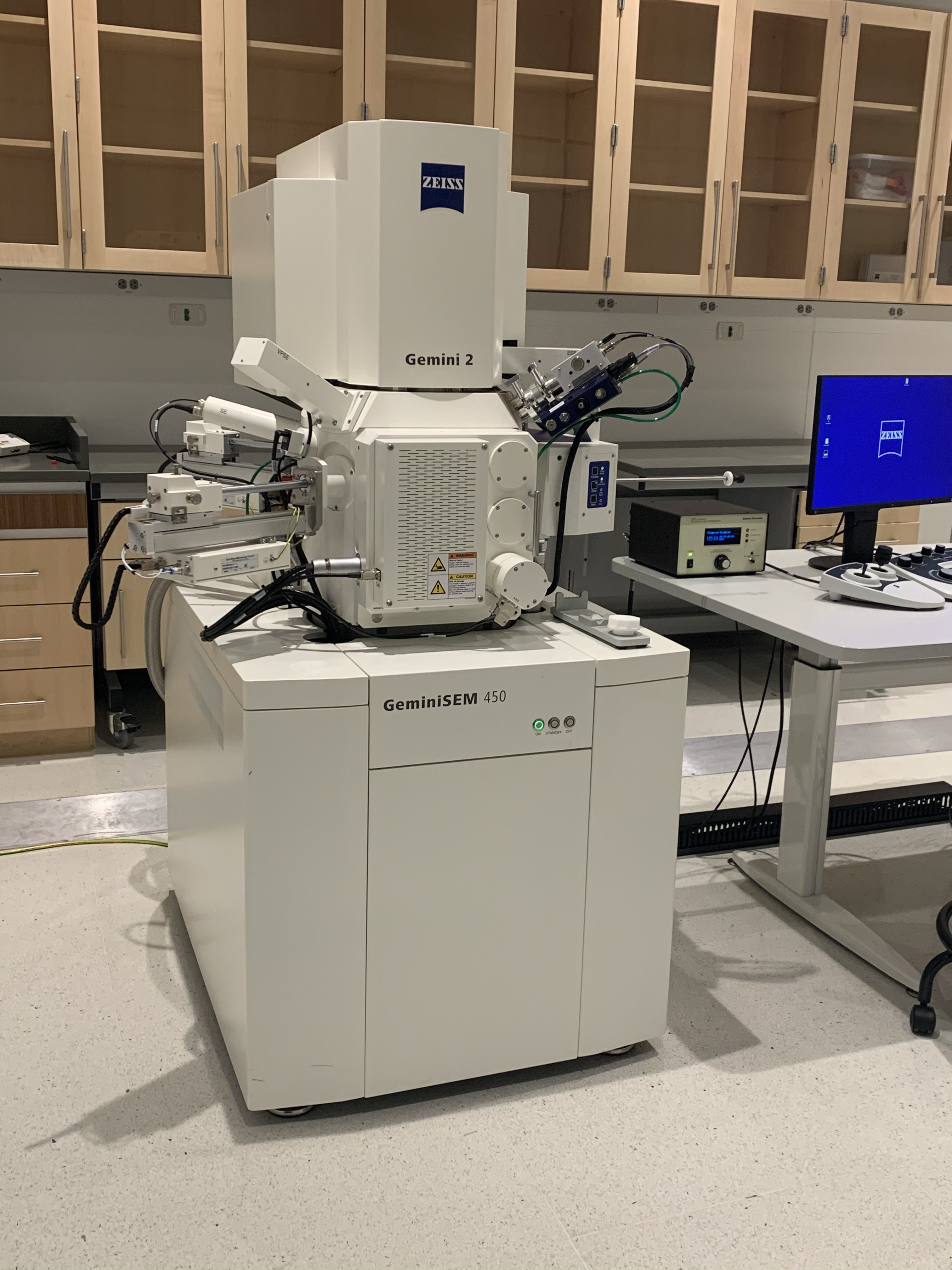
Location: 12-0168 (MIT.nano basement)
Lunch will be provided to registered participants, sponsored by Zeiss

There will be an image contest during lunch. We invite you to submit your best image taken using the Zeiss field emission SEMs at MIT.nano for a chance to win a pair of Zeiss binoculars. Please provide a short description of your image and the imaging conditions.

Register for this talk

ABSTRACT

9:30AM-10:15AM
What to like about imaging with Gemini optics in ZEISS field-emission SEMs
Sandip Basu, Product Marketing Manager, Carl ZEISS Microscopy

Join us as we unravel the transformative potential of surface-sensitive imaging in unlocking new frontiers across various scientific disciplines.

In recent years, the significance of surface-sensitive imaging has surged within the realm of electron microscopy. Understanding when, why and how to image surfaces at low beam energy without compromising resolution integrity and repeatability is crucial for many application fields. 

In this presentation, we will delve into the essential nuances of achieving reliable, repeatable low-voltage imaging, alongside exploring pivotal examples to illuminate its practical applications. We'll analyze the primary challenges inherent in attaining optimal resolution and harnessing unique contrast mechanisms that benefit low-voltage imaging. Moreover, we'll navigate through the intricacies of implementing these techniques within Zeiss field-emission SEMs, contextualizing their relevance across diverse domains such as nanofabrication, energy, healthcare, and semiconductor applications. 
 

10:15AM-11:30AM
Advanced imaging modes in ZEISS field-emission SEMs
Jeff Marshman, Sr. Applications Engineer, Carl ZEISS Microscopy
Anthony Lisi, Product Applications Sales Specialist, Carl ZEISS Microscopy 

Advanced imaging modes have become increasingly important in the field of scanning electron microscopy (SEM). Zeiss field emission SEMs offer a range of high-resolution imaging techniques, including a selection of BSE imaging, high-contrast high-resolution imaging in variable pressure (VP) mode, high-angle annular dark field (HAADF) imaging in STEM mode, and cathodoluminescence (CL).

In this presentation, we will discuss how the beam stability and ease-of-use in switching between imaging and analytics mode in the Zeiss FE-SEMs with dual-condenser electron optic column help in better detection efficiency for energy dispersive X-ray spectroscopy (EDS), and electron backscatter diffraction (EBSD). These techniques allow for the characterization of materials at a micro- and nanoscale, providing detailed information on composition, crystal structure, and morphology. 

In addition, Zeiss field emission SEMs offer the ability to perform in situ experiments, such as heating or cooling samples, to observe dynamic changes in material properties. These advanced imaging modes are critical for researchers in a variety of fields, including materials science, nanotechnology, and biology.

11:30AM-12PM
In Situ SEM Mechanical Characterization of 3D Micro-Architected Materials
James U. Surjadi, Carlos M. Portela, Department of Mechanical Engineering, Massachusetts Institute of Technology, Cambridge, MA, USA

Micro-architected materials represent a new paradigm of materials which provide a pathway to defy the limitations of traditional monolithic materials through their engineered internal microstructures, allowing them to exhibit unique and extreme properties, such as high strength at ultralow densities or large ductility/stretchability from brittle constituents. However, understanding their mechanical response is not trivial, owing to their complex and micro/nano-scale features. Our in situ SEM nanomechanical testing setup serves as a powerful tool, enabling us not only to visualize their deformation behavior during mechanical loading (e.g., compression, tension) but also to capture corresponding force-displacement curves. This capability provides us with the means to conduct a comprehensive analysis of their mechanical properties. One example of such analysis, impossible without in situ SEM mechanical characterization, is that of our recently proposed 3D woven micro-architected materials. These materials are unique, as they are compliant and highly stretchable (up to 10 times more stretchable than its constituent bulk material), but their mechanics involve numerous frictional self-contact due to entanglements between the woven fibers. In situ mechanical testing enables us to observe how these complex architected materials deform, making it possible to model and optimize the design of these architectures. Overall, visualizing and understanding the mechanical response of these micro-architected materials could potentially open new avenues for the creation of unique materials such as flexible glass/ceramics/semiconductors, ultra-light metals with rubber-like response, and scalable nanomaterials for next-generation engineering devices.

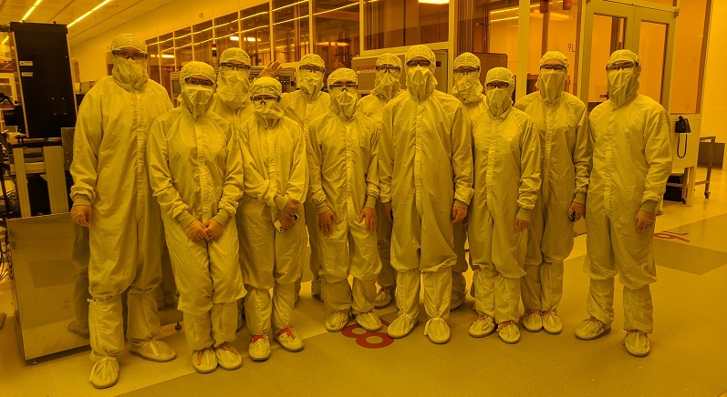
12:00PM-1PM Lunch (sponsored by Zeiss) and image contest 

1PM-4PM Hands-on Demonstration: Best practices for superior imaging and analytics using ZEISS field-emission SEMs 
Jeff Marshman, Sr. Applications Engineer, Carl ZEISS Microscopy